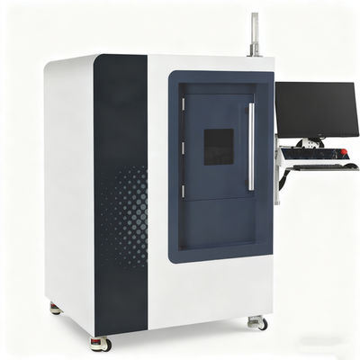
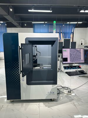
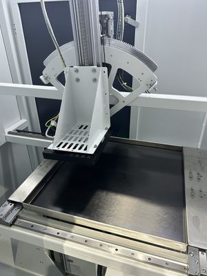
Automatic Defect Detection X-ray Inspection Machine for Electronic
Application Field:
X-ray inspection equipment is mainly applied in the following professional fields:

1. Electronic manufacturing and semiconductor industry
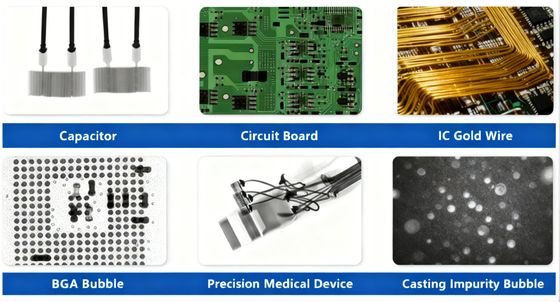
In the production of integrated circuits (IC), printed circuit boards (PCB), and electronic components (such as capacitors, inductors, and connectors), real-time X-ray imaging technology is utilized It can accurately detect internal packaging defects of chips (such as poor gold wire bonding, voids in plastic encapsulation layers), PCB solder joint quality (false soldering, bridging, insufficient solder), and internal structural abnormalities of semiconductor packaging (such as chip offset, package cracking), meeting the quality control requirements for "zero defects" of precision electronic components in fields such as consumer electronics and industrial electronics.
2. The automotive and auto parts industry
For key automotive components (such as engine blocks, transmission valve bodies, and sensor housings), the penetrating power of X-rays is utilized to detect internal pores, cracks, and inclusion defects. For automotive electronic modules (such as on-board PCBS and sensor modules), the reliability of soldering and the integrity of the internal structure can be inspected to ensure the safe operation of the entire vehicle's electrical system, meeting the strict requirements of the IATF16949 quality management system in the automotive industry for component testing.
3. New energy (lithium battery/photovoltaic) industry
In the field of lithium batteries, inspecting the alignment of the electrode sheets of power battery cells, the wrinkles of the separator, internal short-circuit hazards (such as metal foreign objects piercing the separator), and the welding quality of the cells in the PACK is one of the core devices for "safety performance verification" of lithium batteries from the research and development to mass production stage.
In the photovoltaic field: Non-destructive testing is conducted on hidden cracks, fragments of photovoltaic cells and modules, as well as internal bubbles and foreign objects in the packaging layer to ensure the power generation efficiency and service life of photovoltaic products.
4. Aerospace and high-end manufacturing industries
In the production of aerospace precision components (such as aero engine blades and hydraulic system components), detect internal microscopic defects (such as abnormal grains and microcracks); For high-end industrial castings (such as valves and pump bodies), casting defects (shrinkage cavities, sand holes) are inspected to ensure the reliability and safety of high-end equipment.
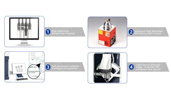
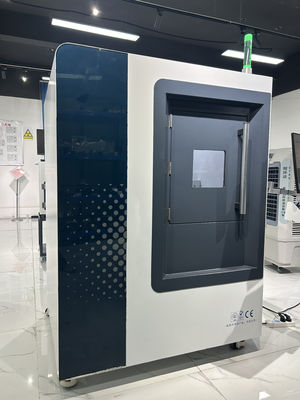
This type of equipment, with its high-resolution X-ray imaging and digital detection and analysis system, has become a key technical device for various industries to achieve "full-process quality traceability" and "precise defect control".
Related Parameters:
| X-ray Source |
Model |
ZL-4009-G740 |
ZL-4009-G750 |
ZL-4009-G751 |
| Type |
Closed type |
Closed type |
Closed type |
| Optical tube voltage |
90kv |
90kv |
130kv |
| X-ray tube current |
90 microns |
90 microns |
300μm |
| Maximum output power |
8W |
8W |
39W |
| Focus size |
5-15um |
5-15um |
5-15um |
| Imaging Unit |
Pixel size |
85um |
| Pixel matrix |
1536x1536 |
| Imaging area |
130.56mmX130.56mm |
| Maximum spatial resolution |
5.5LP/mm |
| Imaging speed |
1-7S |
| Overall machine Parameters |
Overall machine dimensions |
970mm(L)*1720mm(W)*1810mm(H) |
| Overall weight of the machine |
800KG |
| Overall machine power |
250W |
| Power supply |
AC110-240V 50/60Hz |
| Operating temperature |
0-50℃ |

 メッセージは20〜3,000文字にする必要があります。
 メールを確認してください!
  メッセージは20〜3,000文字にする必要があります。
 メールを確認してください!


